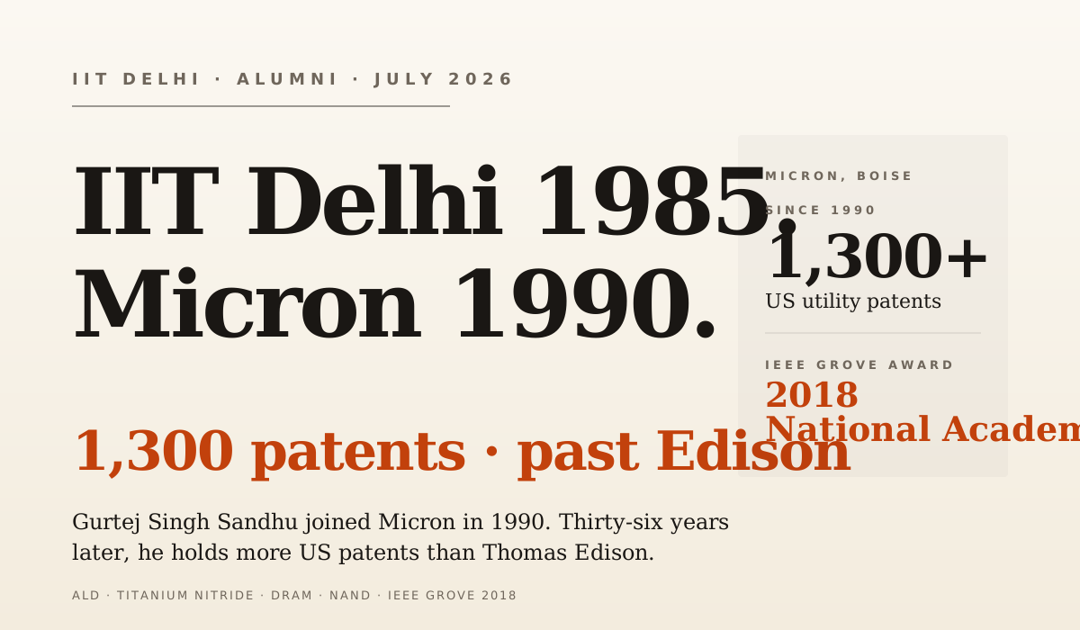
Gurtej Sandhu: The IIT Delhi Alum Who Out-Patented Edison
An M.Tech from IIT Delhi walked into a Boise, Idaho DRAM fab in 1990 and quietly out-invented Thomas Edison. This is the story of Gurtej Singh Sandhu, the Micron Fellow who redesigned how the world stores information.
Is Gurtej Sandhu the world's most prolific inventor?
What did Gurtej Sandhu actually invent at Micron?
Has Gurtej Sandhu received the IIT Delhi Distinguished Alumnus Award?
Why do Reddit IITians care about Gurtej Sandhu in 2026?
May 1985. A 24-year-old with a fresh Master's in Physics from Guru Nanak Dev University, Amritsar, walked out of the M.Tech electrical engineering programme at IIT Delhi with a decision to make. Stay in India, where semiconductor manufacturing did not exist, or head to Chapel Hill, North Carolina, for a PhD in Physics. He chose Chapel Hill. Five years later, Gurtej Singh Sandhu joined a scrappy Boise, Idaho memory company called Micron Technology as a process engineer. He is still there. He now holds 1,432 US utility patents (Micron and IIT Delhi's alumni association pinned the figure at 1,382 in earlier disclosures), roughly 2,211 worldwide, and became the first Indian-born inventor to cross the count Thomas Edison set in 1931. His most-cited patent has been referenced by Samsung, Huawei and every other memory house on earth. Almost nobody in India knew his name until r/IITDelhi posted about him on 24 July 2026. This is the arc.
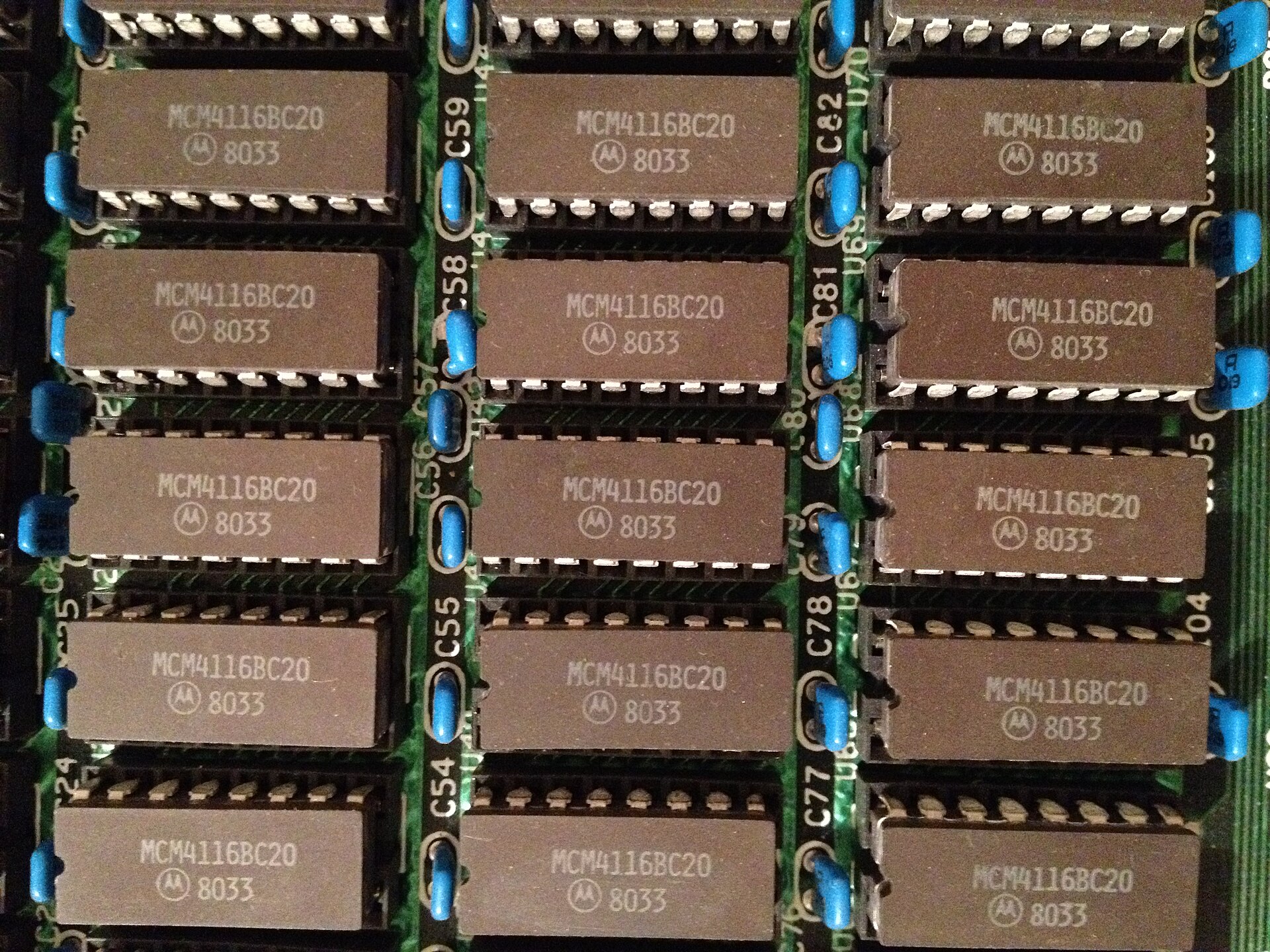
A 16K DRAM chip array — the memory-manufacturing domain where Sandhu's ~1,300 patents live. Photo: Arnold Reinhold, CC BY-SA 4.0 via Wikimedia Commons.Editorial poster · IITian Vibes
Chapter 1: Amritsar to Hauz Khas
Gurtej Singh Sandhu was born in London on 24 October 1960. His parents, Sarjit and Gurmit Sandhu, were both PhD graduates from the University of London. His father would later become a chemistry professor at Guru Nanak Dev University in Amritsar. The family moved back to India in 1963, when Gurtej was three. He grew up in Amritsar, spoke Punjabi at home, and did his Master's in Physics (Honours) at his father's own university before he ever set foot in Delhi.
He arrived at IIT Delhi around 1983 for the M.Tech in Electrical Engineering. This detail matters: he was not an IIT undergrad. He was a physics postgraduate who came to IIT for the applied bit, the part where you translate quantum mechanics into a fabrication process. His two years in Hauz Khas overlapped with the first serious wave of Indian VLSI research. That was the same era that produced the Semi-Conductor Complex Limited (SCL) at Mohali and India's short-lived attempt at a domestic fab. Sandhu completed the M.Tech in 1985. The IIT Delhi alumni association lists him as batch of 1985, Electrical Engineering, M.Tech.
What happened next was the standard 1985 story for anyone with a physics-plus-EE combination and no fab to work in. He applied to American graduate schools. The University of North Carolina at Chapel Hill offered a PhD in Physics with a solid-state materials focus. He took it. In his own telling to Global Indian magazine, his father's advice at that point was blunt: do not pursue chemistry. Find your own vision. Sandhu picked thin films.
Five years later, PhD in hand, he had two offers on the table. Texas Instruments in Dallas, the safe blue-chip semiconductor job. And Micron Technology in Boise, Idaho, a twelve-year-old startup founded in the basement of a Boise dentist's office in 1978 by four engineers with money from potato billionaire J.R. Simplot. Micron had just gone public on the NYSE in November 1990. It was tiny. He picked Micron. He would later tell interviewers he did it for the hands-on invention opportunities: at TI he would be one process engineer among hundreds; at Micron he would touch the actual silicon.
Thirty-six years later, he has not left.
Chapter 2: The titanium problem
Micron in 1990 was a memory company fighting for its life. Japan's DRAM producers, Hitachi, Toshiba, NEC, controlled more than half the world's market. The US industry had already lost the 64K DRAM race a decade earlier. Micron's survival strategy was crude and brilliant: build DRAM chips cheaper than the Japanese, one process improvement at a time. That meant obsessing over every step of the fab flow. Every deposition, every etch, every anneal.
Sandhu, hired as a process engineer, walked into a specific problem within months of joining. When you deposit a metal contact layer on a silicon chip, exposure to oxygen during the process forms a native oxide at the interface. Native oxide is resistance. Resistance is heat and power drain. On a DRAM cell that has to switch billions of times per second, a few extra ohms of contact resistance is a spec failure. Existing physical vapour deposition of titanium was fast but oxygen-hostile: you moved the wafer through air, oxide formed, contacts degraded.
Sandhu's early breakthrough, described by his Micron bio and by the Boise State announcement of his 2018 IEEE Grove Award, was a chemical vapour deposition process for titanium and titanium nitride that never let the wafer see oxygen. CVD Ti/TiN. It was not glamorous. It did not have a marketing name. It became the industry standard for making DRAM contacts, and it is still in production at Micron in 2026, thirty-plus years after he filed the first patents.
That is the pattern with Sandhu. His inventions are not products you can buy on Flipkart. They are steps inside the fab flow. On the r/IITDelhi thread from 24 July 2026, commenter u/intelligentdope asked, "do u know any product made by him." Another commenter, u/Scared_Land_5667, answered the question exactly right, at four upvotes and no fanfare:
"He didn't make a single consumer 'product.' His patents are process technologies licensed to Micron for chip manufacturing, not standalone products."
Which is the whole point. Every SSD in an iPhone. Every DRAM module in a Windows laptop. Every high-bandwidth memory stack sitting next to an Nvidia H100 GPU. Somewhere in the fab flow, Sandhu's process is on the wafer.
Chapter 3: The insight that became a decade of scaling
Around 1999, DRAM hit a wall. The cell capacitor was shrinking faster than the dielectric material could keep up. Silicon dioxide, the workhorse insulator, was too thin at the 90-nanometre node. Electrons tunnelled through it. Data leaked. You could not hold a stored bit long enough to read it.
The industry knew the answer in principle: high-k dielectrics. Materials like hafnium oxide have a much higher dielectric constant than silicon dioxide, so you can hold the same charge with a physically thicker (safer) layer. But depositing high-k films evenly over the vertical trenches of a modern DRAM capacitor is a nightmare. Line-of-sight sputter deposition puts too much material on the top and too little at the bottom. You need a process that deposits one atomic layer at a time, conformal to the surface geometry.
That process existed. It was called Atomic Layer Deposition (ALD), invented in Finland in the 1970s for electroluminescent displays. Nobody had made it work economically for high-volume memory. In 2000, Sandhu and a colleague named Trung T. Doan started the programme at Micron to do exactly that. As documented on his Wikipedia page and elaborated in IEEE Spectrum's interview, Sandhu initiated the ALD high-k programme for DRAM in that year and drove cost-effective implementation into the 90-nm node.
By the 90-nanometre node, shipping in DRAM around 2004-2006, Micron had ALD high-k running in volume production. Every major DRAM maker followed. Sandhu did not invent ALD; he invented the version of ALD that fits inside a memory fab's cost envelope. That is a specific kind of engineering achievement, and it is why his patent on the technique gets cited by Samsung, SK Hynix and Huawei more than 1,200 times.
Then came pitch doubling. Around 2005, NAND flash memory hit its own scaling wall. The wavelength of the lithography light was longer than the features you needed to print. You could not draw lines finer than the photons could resolve. Sandhu's answer, filed in a series of patents in the mid-2000s, was a self-aligned double patterning trick: draw the coarse pattern, deposit a spacer on the sidewalls, then etch away the original pattern and use the spacers as the new mask. Effective feature pitch: halved. NAND could keep scaling into the 3X-nm node without new lithography hardware.
That trick, pitch doubling or self-aligned double patterning, is why the SSD in your laptop got cheaper every year from 2007 to 2015. When IEEE Spectrum interviewed him a few years later, Sandhu was already looking past it:
"Moore's Law is dead in some cases. For example, in NAND, planar scaling died a few years ago, so we went to 3D NAND. Moore's Law's decline was inevitable. The question is, what do we do next? It opens up new opportunities for innovation."
Chapter 4: The night Edison fell
Thomas Edison held 1,093 US utility patents at his death in 1931. For most of the twentieth century, that number was untouchable. Then things changed. Kia Silverbrook of Australia crossed 4,000 US patents by 2010 with his inkjet printing work. Shunpei Yamazaki of Japan's Semiconductor Energy Laboratory currently sits at over 20,120 patents worldwide, 6,700-plus of them US utility grants, as of March 2025.
So Sandhu is not the world number one. Nobody serious ever claimed that. What he is: the first Indian-born inventor to cross the Edison line, and by 2025 he sits inside the top-10 to top-25 of all-time US utility patent counts, depending on which ranking you accept. The Wikipedia list of prolific inventors, updated to July 2026, has him at rank 22 with 1,435 US utility patents accumulated between 1991 and 2024. Roughly 44 patents per year, every year, for thirty-three years.
Here is the career timeline in one table.
Year
Milestone
Source
1960
Born in London, 24 October, to Sarjit and Gurmit Sandhu
The 2018 IEEE Andrew S. Grove Award citation reads, in full: "For outstanding contributions to silicon CMOS process technology that enables DRAM and NAND memory chip scaling." That is the sentence that captures thirty years of work. The prize is named after Andy Grove, Intel's third CEO and the man who wrote Only the Paranoid Survive. It is the highest US honour in the field.
Cumulative US utility patents
Edison's 1,093 line (1931), Sandhu (Micron), Yamazaki (SEL), 1990 to 2026
1990
2000
2010
2020
2026
1,000
2,000
3,000
5,000
7,000
Edison, 1,093 patents (1931)
Sandhu 1,432
Yamazaki 6,700+
2005: pitch doubling
2000: ALD high-k programme starts
Sources: Wikipedia (List of prolific inventors, Jul 2026); Guinness (Yamazaki, Sep 2025). Chart by IITian Vibes.
Sandhu crossed Edison's 1,093-patent line around 2019 and continues to file. Yamazaki's Japanese SEL portfolio dwarfs both, but on the US utility count Sandhu now sits inside the all-time top 25.
Chapter 5: Why India didn't build him
The r/IITDelhi thread on 24 July 2026 racked up 157 upvotes and 20 comments in 48 hours. It is a small thread by internet standards. But the comment section is the most honest thing I have read about India's semiconductor story this year. The top-voted comment, from u/_sai_raj at eight upvotes, is one sentence.
"There is not a single fab in india. He would have wasted his talent have he stayed in india."
That sentence is technically wrong. SCL Mohali has run a small government fab since the 1980s, and Tata's fab in Dholera and Micron's own $2.75-billion assembly plant in Sanand are under construction under the India Semiconductor Mission. But the spirit is right. When Sandhu made his 1990 decision, India had zero commercial-scale DRAM manufacturing. In 2026, it still has essentially none in production. If he had stayed, there would have been no fab flow to invent for.
Not everyone on the thread agreed with the framing. u/EnigmaticBuddy pushed back at one upvote: "Everybody knows the problem in India, building startups ain't smooth. US has both capital and infra for such stuff." Someone else pointed out the M.Tech-vs-B.Tech snobbery baked into IIT culture, with u/intelligentdope writing at four upvotes:
"kya retard? yahan pr matka kahan se aya, for all I care Mtech students should be more respected. it should only be In india that bachelours student disrespect masters and call names, like wtf. what kind of retardness is this."
The exchange is worth quoting because it exposes a structural bias inside IIT that Sandhu's story pushes against. On the r/IITDelhi thread, one comment (now downvoted) implied he did not count as a real IITian because he was only an M.Tech, not a four-year B.Tech. This is the same bias that makes almost every IIT hall-of-fame list default to undergrad alumni. Sandhu is not on those lists. He should be.
The other useful voice in the thread came from u/Ok-Constant-807, at seven upvotes, and it was directed at the OP:
"kindly refrain from posting Linkedin Larps here, THERE is a reason why ppl open reddit dont make this sub, another linkedin"
Which is its own kind of tell. When a genuine achievement post lands on r/IITDelhi, the default reaction is to accuse the poster of LinkedIn-style bragging. Sandhu's actual work, hidden inside process technology that nobody outside a fab sees, does not fit the achievement grammar the sub is used to. He is not a founder with a valuation. He is not a professor with a paper. He is a process engineer with 1,382 patents and no personal brand. The sub struggled to parse him.
"I don't do patents for the sake of patents. The patent is an output of an activity."
He is also unusually democratic about invention. From Global Indian:
"We all have this capability to find a creative solution. It has no bearing on what your education is, what your background is, who you are. Stay open, stay curious, explore it."
His view of the next decade of computing is memory-centric, not compute-centric, a specific disagreement with the CPU-and-GPU-obsessed industry mainstream. From IEEE Spectrum: "We've been computing the same way for last 50 years, and it's not sustainable. Instead of being compute-centric we need to be memory-centric." And on the wildest edge of his imagination: "In principle you could have a teaspoon of DNA and the entire world's info as it exists today could be fit into it."
He has spent fifteen-plus years mentoring engineering students at Boise State University and helped launch its PhD programme in Materials Science and Engineering. He plays basketball and table tennis. He has never been on the cover of an Indian news magazine before 2019.
Chapter 7: What current IITians can actually take from this
Sandhu's story is a bad template if you're looking for a viral one. He didn't found a unicorn. He never IPO'd. He is not on a Forbes list. He picked one company at 30 and stayed for 36 years. But strip the profile down and there are five specific things worth stealing.
One: pick a chokepoint, not a product. Sandhu did not invent a phone or a chip. He invented the deposition step inside the fab that everyone else needs. Chokepoint technology compounds harder than product technology, because every downstream product depends on it. Look at where your industry has a physical or process bottleneck and stand there.
Two: an M.Tech is not a consolation prize. He did not do a B.Tech at IIT. He did a Master's in Physics, then an M.Tech, then a PhD. The M.Tech was the specific piece that turned his physics into engineering. IIT's B.Tech culture is dominant enough that this bears repeating: postgraduate degrees at IIT are a serious path, not a compromise, and the alumni networks recognise them as such, witness the 2023 Distinguished Alumnus Award.
Three: geography matters. He moved to Boise, Idaho, in 1990 because that is where the fab was. He did not try to work on DRAM from Bangalore. If your problem lives in a specific city, live in that city. This is uncomfortable career advice for anyone romantic about staying home, but it is what the actual data says.
Four: patents are a residue, not a goal. "The patent is an output of an activity." If you are optimising for patent count, you are optimising the wrong thing. Optimise for problems solved. The patents will show up.
Five: stay past year seven. Every big Sandhu invention happened after his tenth year at Micron. CVD Ti/TiN in the early 1990s was a fast win. ALD high-k took a decade of programme building starting in 2000. Pitch doubling took another five years after that. The compound returns on a single-company career are grotesquely under-appreciated in the current tech-job-hopping culture. He is 65 years old and still filing.
If you are an IIT Delhi undergrad in July 2026 reading this, you can walk twenty minutes from Vindhyachal hostel to the Bharti School of Telecom Technology, where the semiconductor labs are. India in 2026 is finally trying to build the fab infrastructure Sandhu had to leave to find. Sanand's assembly plant will ramp to hundreds of millions of chips a year by 2027. Tata's Dholera fab is under construction. The India Semiconductor Mission has committed roughly $15 billion. There will be process engineering jobs at home for the first time in Sandhu's lifetime. Someone from the IIT Delhi M.Tech Class of 2027 might be the person who does for India what Sandhu did for Micron. If that person exists, they are probably reading a Reddit thread right now.
And they can wear the campus with a bit of pride while they figure it out. Our IIT Delhi hoodies are made for the walk from Vindhyachal to the semiconductor lab and back. Sandhu did that walk in 1984. It still counts.
Last updated: July 2026. By Arun Raghav S, Co-founder, IITian Vibes · B.Tech, IIT Jodhpur.
Photo: Press Bureau of India, Government of India, GODL-India via Wikimedia Commons.
Frequently asked questions
How many patents does Gurtej Sandhu hold?
Wikipedia's 2026 tally lists 1,432 US utility patents and roughly 2,211 worldwide. IIT Delhi's alumni association and Micron's Legal Department pinned the count at 1,382 in earlier disclosures. Either way, he crossed Thomas Edison's 1,093 count around 2019 and is still filing.
Which IIT and branch did Gurtej Sandhu attend?
He completed his M.Tech in Electrical Engineering at IIT Delhi in 1985, after a Master's in Physics from Guru Nanak Dev University, Amritsar. He then moved to the US for his PhD in Physics at the University of North Carolina, Chapel Hill (1990).
Is Gurtej Sandhu the world's most prolific inventor?
No. He is the most prolific US-based inventor of Indian origin, but the global crown belongs to Japan's Shunpei Yamazaki (over 20,000 patents worldwide, 6,700+ in the US). Sandhu was ranked seventh worldwide when he crossed Edison; more recent 2026 rankings place him around 22nd on US utility patents alone.
What did Gurtej Sandhu actually invent at Micron?
Three big things. A titanium/titanium-nitride CVD coating (early 1990s) that made oxygen-free contacts possible in DRAM. Atomic Layer Deposition of high-k dielectrics, which he started with Trung T. Doan around 2000 and shipped in 90-nm DRAM. And the pitch-doubling patterning technique (mid-2000s) that scaled NAND flash into the sub-30nm era.
Has Gurtej Sandhu received the IIT Delhi Distinguished Alumnus Award?
Yes. IIT Delhi conferred the Distinguished Alumnus Award on him in 2023 for his contributions to semiconductor technology and atomic layer deposition. He also received the IEEE Andrew S. Grove Award (2018), the FLOGEN Fray International Sustainability Award (2022), and the Vigyan Ratna at Panjab University's convocation from President Droupadi Murmu in March 2025.
Why do Reddit IITians care about Gurtej Sandhu in 2026?
Because he is the counter-example. When r/IITDelhi celebrated him on 24 July 2026, the top-voted debate wasn't about the patents. It was about whether he'd have wasted his talent had he stayed in India. "There is not a single fab in india," one commenter wrote. The thread became a referendum on India's semiconductor gap.